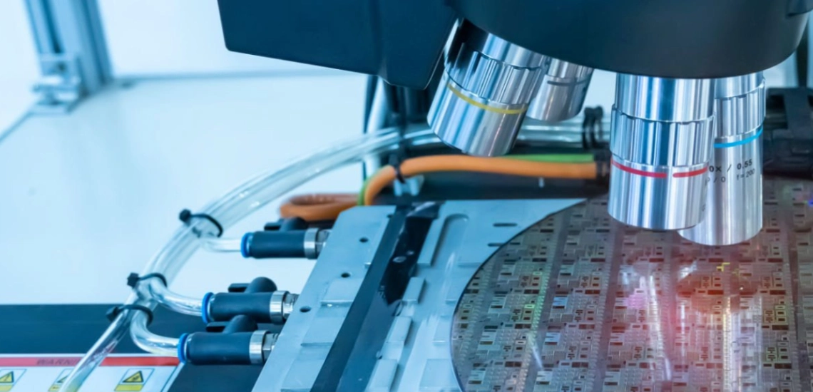
The relentless march of technology is a testament to human ingenuity. Behind every tiny transistor and minuscule microchip lies a world invisible to the naked eye. At the heart of this microscopic exploration lies a potent tool – the Scanning Electron Microscope (SEM). Semiconductor fabrication facilities, or fabs, rely heavily on this investigative device to ensure the precise engineering of electronic components. This article delves into the intricacies of the SEM and its indispensable role in semiconductor fabs.
Understanding the Scanning Electron Microscope (SEM)
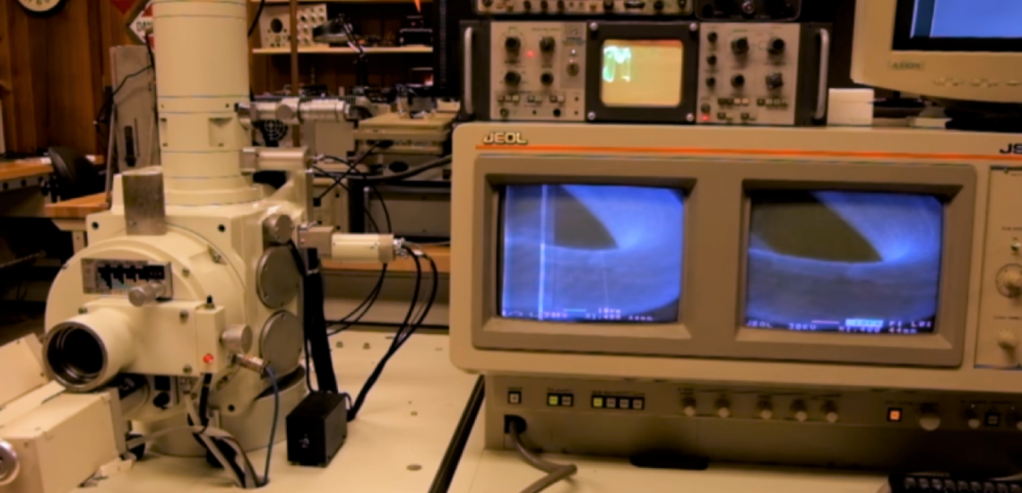
The SEM is an electron microscope that produces images of a sample by scanning its surface with a focused beam of electrons. Unlike traditional light microscopes, SEMs have the ability to delve into the nanoscale, unveiling details as small as a few nanometres in size.

The primary components of an SEM include:
- Electron Gun: Generates the primary electron beam.
- Electromagnetic Lenses: Focus the electron beam onto the sample.
- Scanning Coils: Control the scanning motion of the electron beam.
- Detectors: Capture secondary or backscattered electrons emitted from the sample.
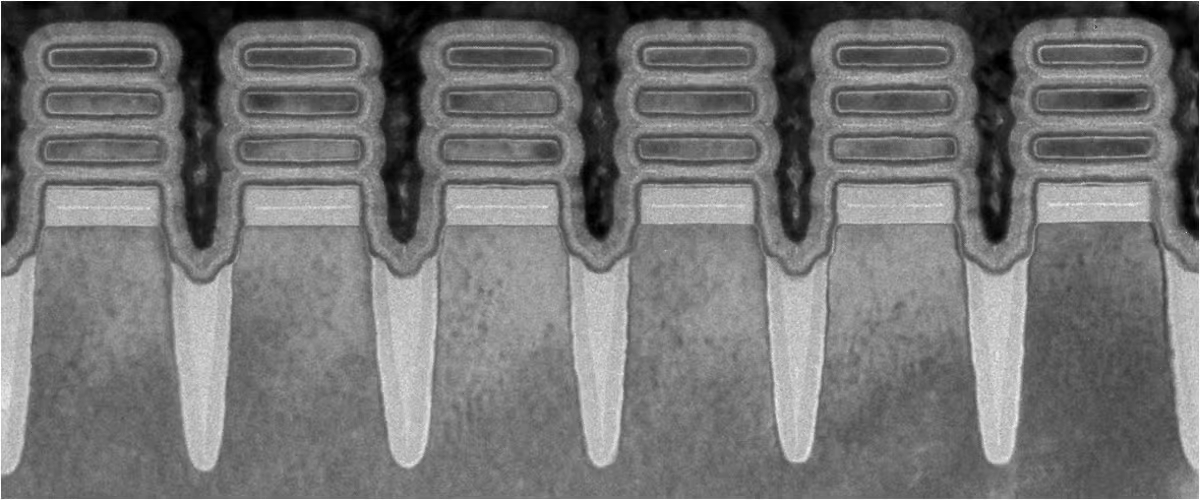
The electron beam interacts with the atoms in the sample, producing various signals that contain information about the sample’s surface topography and composition. The SEM’s detectors capture these signals to create a detailed image of the surface.
Applications in Semiconductor Fab
The microscopic nature of semiconductors necessitates stringent quality control and process monitoring. Here’s how SEMs contribute to the semiconductor manufacturing landscape:
Defect Analysis
SEMs play a crucial role in defect analysis by identifying and characterizing failures at the microscopic level. Understanding the nature of defects helps in optimizing the manufacturing process and enhancing the yield.
Metrology
Accurate measurements of critical dimensions, such as the width and height of semiconductor structures, are paramount. SEMs offer the high-resolution imaging and measurement capabilities required for this crucial task.
Material Analysis
Through techniques like Energy Dispersive X-ray Spectroscopy (EDS) integrated with SEM, it’s possible to analyze the elemental composition of materials, which is critical for ensuring the purity and consistency of semiconductor materials.
Process Development
As semiconductor technology continues to advance, process development becomes increasingly complex. SEMs provide invaluable insights into the interaction between materials and processes at the nanoscale, aiding in the development of new manufacturing techniques.
Lithography Process Control
The lithography process, which involves patterning the semiconductor material, is fundamental to semiconductor manufacturing. SEMs help in monitoring and controlling this process to ensure the precise replication of patterns.
Conclusion
The SEM is more than just a microscope; it’s a gateway to the microcosm that holds the secrets of modern electronics. By enabling precise analysis and control at the nanoscale, SEMs are indispensable tools in semiconductor fabs, pushing the boundaries of what’s possible in the ever-evolving field of semiconductor technology. Through continued advancements in SEM technology, we inch closer to unlocking new horizons in the realm of micro and nanotechnology, propelling the semiconductor industry into a new era of innovation.