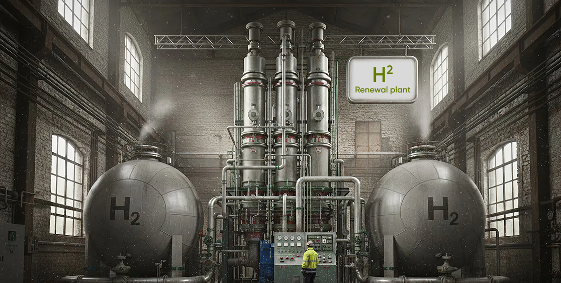
Emerging Memory Technologies: Revolutionizing Semiconductor Fabs

Emerging Memory Technologies: Revolutionizing Semiconductor Fabs

The relentless evolution of the semiconductor industry is driven by one fundamental principle: memory. Memory technologies are the unsung heroes behind the digital age, underpinning everything from your smartphone’s data storage to supercomputers’ efficiency. As demand for faster, more reliable, and energy-efficient memory surges, a new wave of emerging non-volatile memory technologies is poised to reshape semiconductor fabs and enhance our digital experiences.

Emerging Technologies in Semiconductor Packaging Industries

Emerging-Technologies

In the fast-paced realm of technology, the semiconductor packaging industry plays a pivotal role, not only providing electrical connections to integrated circuits (ICs) but also facilitating heat dissipation and shielding chips from mechanical damage and chemical contamination.

Sustainability in Semiconductor Fabs: A Green Revolution in Silicon 

sustainability_in_semiconductor_fab

In an era of rapidly advancing technology, the global semiconductor industry finds itself at the heart of innovation. Its products, the tiny silicon chip that power our digital world, have enabled everything from smartphones to self-driving cars. However, this technological progress has come at a price – a significant environmental footprint.

Silicon Carbide (SiC): The Future of the Compound Semiconductor Industry

Silicon_Carbide_Future_CSI

In the burgeoning landscape of the semiconductor industry, Silicon Carbide (SiC) emerges as a promising material, unveiling opportunities for superior electronic performance at a competitive cost. The industry’s relentless pursuit for enhanced efficiency, higher operating temperatures, and reduced system costs has brought SiC into the spotlight, making it a frontrunner in the compound semiconductor sector.

Unveiling the Microcosm: The Scanning Electron Microscope in Semiconductor Fabs

Unveiling the Microcosm

The relentless march of technology is a testament to human ingenuity. Behind every tiny transistor and minuscule microchip lies a world invisible to the naked eye. At the heart of this microscopic exploration lies a potent tool – the Scanning Electron Microscope (SEM). Semiconductor fabrication facilities, or fabs, rely heavily on this investigative device to ensure the precise engineering of electronic components.

Sneak in to not so known Packaging Engineering

Packaging Engineering

Yes, Packaging engineering is something that not many have heard of but is an important aspect of almost every product that you buy or sell. This is considered a niche area with a question from everyone.

An Insane Work Ethic

ethic

Work ethic is a set of standards of behavior and beliefs that drives our attitude towards what is and what is not acceptable.It depends on our personal views, motivation, social, organizational, and cultural set-up. It’s a value based on the hard work and diligence and strengthens the belief in the moral benefit of work and its ability to enhance character.

Gallium Nitride – The Dark Horse of Semiconductor Industry

Gallium Nitride

Group III-Nitride materials are the class of compound semiconductor consisting of elements namely Gallium, Indium and Aluminium with Nitrogen. The nature has blessed these semiconductor alloys system with persisting direct band gap. In today’s world these materials have proven the backbone of solid-state lighting application by achieving bright blue LEDs. The III-V blue LED technology has opened enormous new markets that were not accessible before.