
In the semiconductor manufacturing domain, precision is not just a preference; it’s a mandate. The machinery involved operates at scales where even the slightest deviation can result in significant consequences. Calibration and metrology emerge as linchpin processes, guaranteeing the accuracy and reliability of semiconductor manufacturing equipment. Here’s a concise exploration of their critical roles:
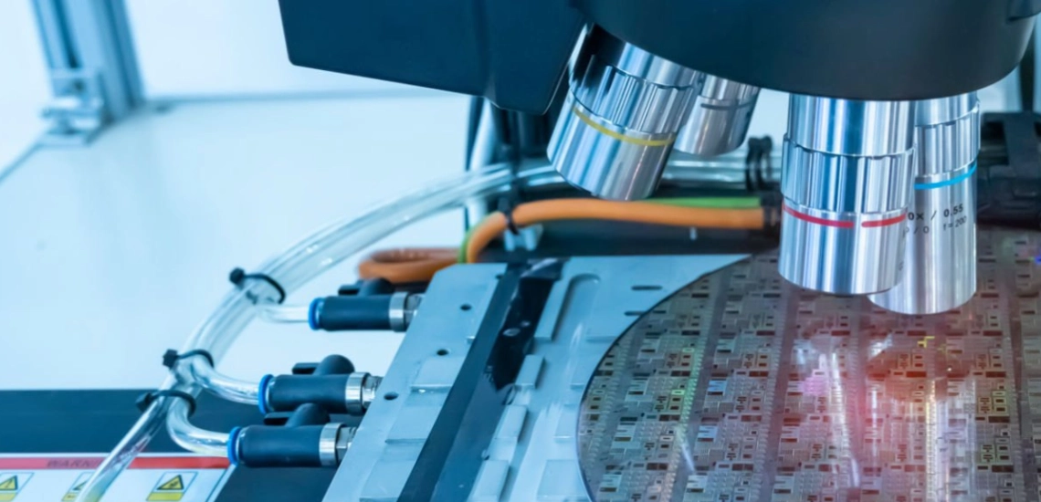
- Wafer Inspection Tools: Wafer inspection tools, including scanning electron microscopes (SEM) and optical inspection systems, are pivotal for defect identification in semiconductor material. Calibration ensures the meticulous adjustment of these tools, preserving the integrity of the inspection process by accurately detecting and categorizing defects.
- Laser Interferometry for Lithography Equipment: In the realm of lithography equipment, where an extraordinary level of precision is demanded, laser interferometry takes center stage for calibration. This technique measures the displacement of mirrors within lithography tools, guaranteeing microscopic precision alignment of projected patterns onto semiconductor material.
- Atomic Force Microscopy (AFM) for Surface Metrology: Surface metrology, especially crucial in semiconductor processes like etching and deposition, relies on tools such as Atomic Force Microscopy (AFM). Calibration of AFM involves adjusting parameters to ensure accurate readings of nanoscale surface features. This guarantees precise control over material removal and deposition processes.
At the heart of semiconductor manufacturing lies a dual powerhouse: calibration and metrology. Calibration meticulously fine-tunes tools, ensuring flawless accuracy, while metrology, the scientific discipline of precise quantification, acts as the guardian of manufacturing standards. Together, they fortify quality assurance, enhance tool longevity, guarantee compliance, and drive the relentless pursuit of accuracy and efficiency in semiconductor processes.
1. Precision at the Core: Calibration is the meticulous fine-tuning of manufacturing tools to a reference standard, ensuring impeccable accuracy in their performance. Simultaneously, metrology is the scientific discipline that delves into the precise quantification and standardization of these measurements.
2. Quality Assurance: Robust calibration protocols are indispensable for maintaining the accuracy of tools, ensuring they operate within high-quality manufacturing standards. Periodic metrological checks further validate tool precision, reinforcing the assurance of top-tier manufacturing.
3. Tool Longevity: Regular calibration acts as a preventative measure, averting premature wear and tear, and thus, extending the operational life of costly equipment. Simultaneously, metrological assessments contribute significantly to tool reliability, ensuring consistent performance over time.
4. Compliance Standards: Adherence to calibration standards is paramount, ensuring compliance with rigorous industry regulations. In tandem, metrology plays a crucial role in guaranteeing that tools meet and exceed industry standards, aligning seamlessly with regulatory requirements.
5. Accuracy in Semiconductor Processes: In semiconductor fabrication, calibration stands as the sentinel of accuracy, particularly in processes like lithography and etching. Simultaneously, metrology assumes a paramount role when dealing with nanoscale precision, a cornerstone of semiconductor manufacturing excellence.
6. Process Optimization: Fine-tuned tools, a product of effective calibration, operate with heightened efficiency, optimizing various manufacturing processes. Metrology contributes valuably to process refinement, allowing continuous improvement in semiconductor manufacturing methodologies.
7. Cost-Efficiency: Calibration serves as a safeguard against costly errors in production by preventing inaccuracies that could lead to expensive mistakes. Moreover, efficiency driven by metrology minimizes resource wastage, contributing significantly to the overall cost-effectiveness of semiconductor manufacturing.
In summary, the synergy of calibration and metrology is the backbone of precision in the semiconductor domain. Their roles extend beyond routine maintenance, influencing the very quality, efficiency, and innovation that define the semiconductor industry’s trajectory. As technology continues to advance, the significance of these processes in maintaining the semiconductor industry’s competitive edge cannot be overstated.