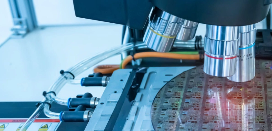
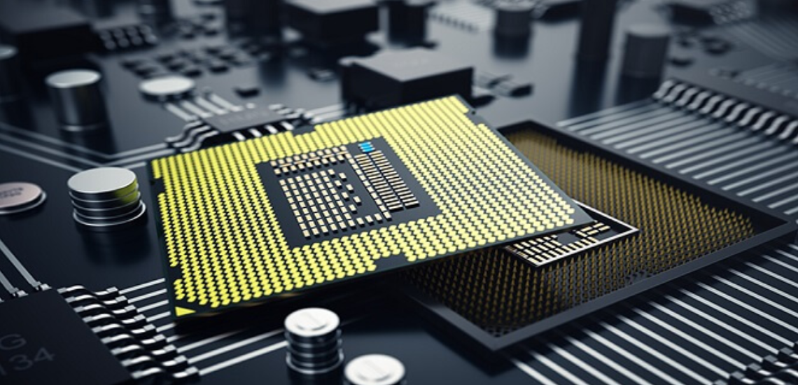
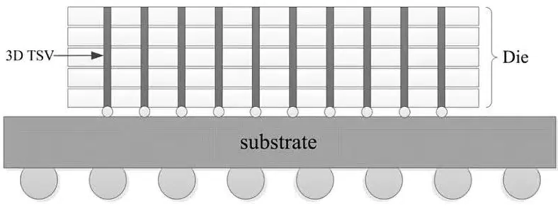
In the fast-paced realm of technology, the semiconductor packaging industry plays a pivotal role, not only providing electrical connections to integrated circuits (ICs) but also facilitating heat dissipation and shielding chips from mechanical damage and chemical contamination. Various innovations have emerged in this domain, driven by the relentless advancement in semiconductor technology. One such innovation is 3D IC Packaging, which enables the stacking and vertical interconnection of silicon wafers or dies using through-silicon vias (TSVs), thereby forming a single circuit. This technology enhances performance by minimizing delay and power consumption and provides more functionality in a compact footprint. However, it does present challenges in managing thermal issues due to the compact 3D structure and complexity in manufacturing processes.
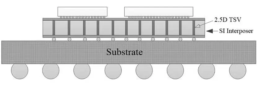
Another groundbreaking technology is Fan-Out Wafer-Level Packaging (FOWLP), which eschews wire bonding, allowing for a larger number of I/O ports while maintaining a sleek, compact size. While FOWLP presents advantages like enhanced electrical and thermal performance, it also introduces challenges such as a high implementation cost and ensuring consistent manufacturing yield. On a similar note, 2.5D IC Packaging utilizes a silicon interposer to facilitate high-speed communication between dies placed side-by-side on a single substrate. It not only facilitates rapid data transfer but also minimizes energy usage by shortening interconnect lengths, albeit at a relatively high production cost and with challenges in heat dissipation.
Meanwhile, Flexible Hybrid Electronics (FHE) merge the merits of flexible electronics with the robust performance of semiconductor devices by integrating chips onto pliable substrates. Despite offering flexibility and reduced weight, ensuring the durability and reliability of flexible structures and developing scalable manufacturing processes remain challenges. Conversely, Panel-Level Packaging (PLP), which processes multiple packages on a larger panel instead of a traditional wafer, promises cost-effective mass production. However, managing panel warpages during processing and establishing standards for panel sizes and processes are hurdles to be overcome.
In an era driven by data, integrating Artificial Intelligence (AI) and Machine Learning (ML) into semiconductor packaging processes is enhancing efficiency, predictability, and reliability through intelligent data analytics and autonomous decision-making. While AI and ML offer the benefits of predictive maintenance and enhanced quality control, ensuring the security and integrity of data, and aligning AI/ML technologies with existing processes present their own set of challenges.
In conclusion, as electronic devices continue to demand smaller, faster, and more efficient components, the semiconductor packaging industry stands at the forefront of innovation, shaping not only its future but also impacting various sectors such as IoT, automotive, and healthcare. The challenges brought about by these advancements offer opportunities for further research and development, propelling the industry towards new breakthroughs. It is vital to recognize that the future of electronics hinges not only on the chips themselves but also on their packaging, ensuring their optimal performance, reliability, and cost-effectiveness.