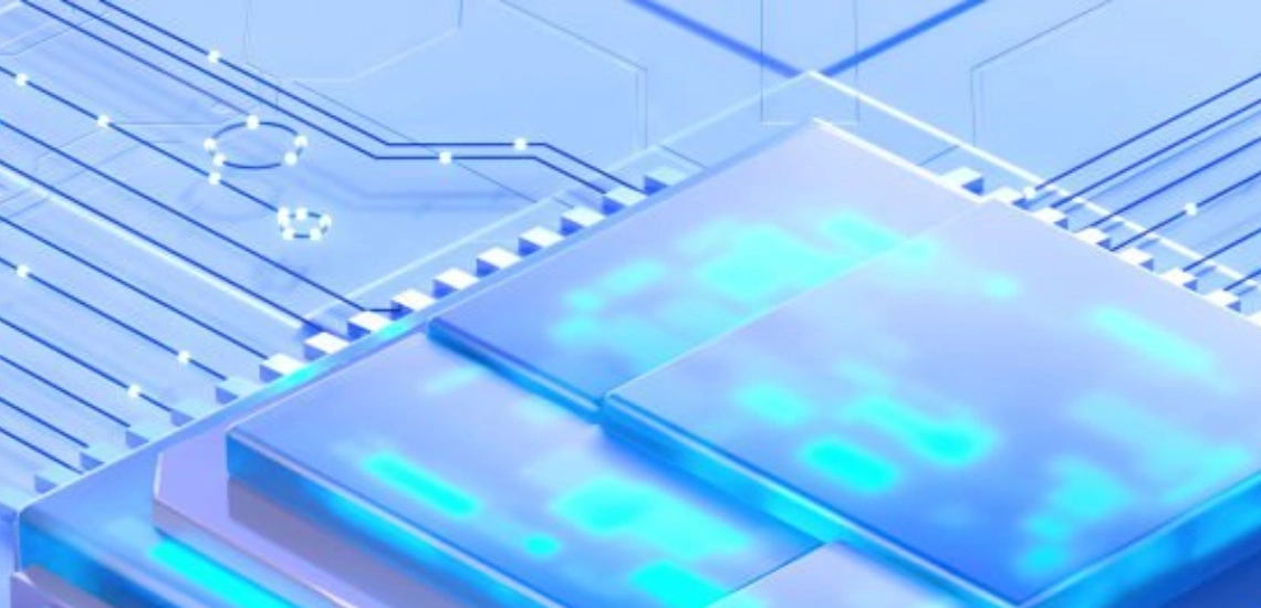

In the dynamic realm of semiconductor fabrication, the continuous evolution of lithography technologies plays a pivotal role in defining the industry’s trajectory. Extreme Ultraviolet (EUV) lithography, hailed as a game-changer, has witnessed remarkable advancements in 2023, illuminating new possibilities for the semiconductor landscape. EUV lithography, operating in the spectral range of approximately 13.5 nanometers, has become the linchpin of cutting-edge semiconductor manufacturing. Its shorter wavelength allows for unparalleled precision in etching intricate patterns onto silicon wafers, overcoming the limitations of traditional optical lithography.
Enhanced Resolution and Miniaturization
One of the key advancements in EUV lithography is the unprecedented enhancement in resolution. The technology now enables the fabrication of semiconductor components with feature sizes reaching unprecedented levels, down to a few nanometers. This breakthrough translates to increased transistor density and, consequently, more powerful and efficient chips.
Increased Throughput and Productivity
The throughput of EUV lithography machines has seen a substantial boost. The introduction of advanced light sources and optics has significantly reduced exposure times, allowing for quicker and more efficient production processes. This increase in throughput directly contributes to higher productivity in semiconductor fabrication facilities.
Overlay Accuracy and Yield Improvement
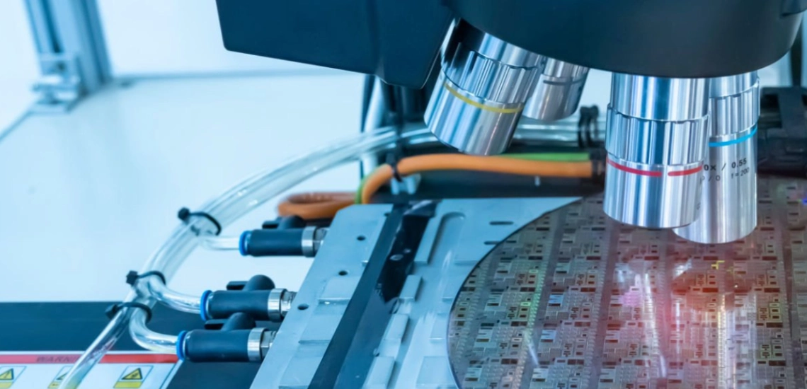
Overlay accuracy, the precision with which successive layers align, has been a historical challenge in lithography. In 2023, EUV lithography has made substantial progress in overcoming this challenge. Improved overlay accuracy ensures higher yield rates, reducing the number of defective chips and enhancing the overall efficiency of semiconductor manufacturing.
Advancements in Light Source Technology
The heart of any EUV lithography system is its light source. Advances in this critical component have been a focal point in 2023. Higher power EUV sources have been developed, leading to increased machine reliability and stability. This, in turn, minimizes downtime and enhances the overall cost-effectiveness of EUV lithography.
Integration of Artificial Intelligence (AI) and Machine Learning (ML)
EUV lithography systems are increasingly incorporating AI and ML algorithms to optimize various aspects of the fabrication process. From predictive maintenance to real-time adjustments in exposure parameters, the integration of smart technologies enhances the overall adaptability and efficiency of EUV lithography.
Impact on Semiconductor Fabrication Industry
- Advanced Node Semiconductor Manufacturing EUV lithography’s advancements are propelling the semiconductor industry into advanced nodes. This transition is critical for developing more energy-efficient, high-performance chips that cater to the demands of emerging technologies such as 5G, artificial intelligence, and the Internet of Things (IoT).
- Cost Reduction and Scalability The increased throughput, improved yield, and enhanced overlay accuracy contribute to a reduction in overall manufacturing costs. As EUV lithography becomes more mainstream, scalability becomes a reality, allowing semiconductor manufacturers to meet the rising demand for innovative and complex microelectronics.
- Innovation in Memory and Logic Devices EUV lithography’s refined capabilities are fostering innovation in memory and logic devices. The technology’s ability to print smaller and denser patterns opens avenues for the development of novel architectures, pushing the boundaries of what is achievable in semiconductor design.
Challenges and Future Prospects
While EUV lithography has undoubtedly made substantial progress, challenges persist. Ensuring a stable supply chain for critical raw materials, further improving machine reliability, and addressing the complexities of defect inspection at smaller nodes are among the challenges that the industry is actively addressing.
Conclusion
The advancements in EUV lithography in 2023 underscore its transformative role in semiconductor fabrication. From enhanced resolution to improved throughput and overlay accuracy, EUV lithography is steering the industry towards a future of more powerful, efficient, and innovative microelectronics. As semiconductor manufacturers embrace these advancements, the stage is set for a new era of technological possibilities.
In a world where the pace of technological evolution defines competitiveness, the strides in EUV lithography illuminate a path towards semiconductor excellence. The semiconductor fabrication landscape, guided by these advancements, is poised to redefine the boundaries of what’s achievable in the digital age.